Dr. Onur Tokel and his research group published a new article on Nature Communications titled: “Laser nanofabrication inside silicon with spatial beam modulation and anisotropic seeding“.
It is featured on the widely read IEEE Spectrum magazine as “Carving Out Nanostructures Beneath the Surface of Silicon: A new laser system makes it possible to build photonic elements inside wafers”.
It is also featured on the international news outlets phys.org and Microsoft Start as “Researchers achieve unprecedented nanostructuring inside silicon”.
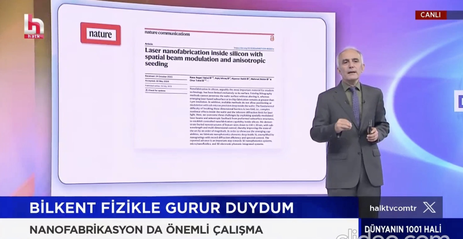
It was also featured in a program by Emin Çapa on a national TV channel (you can watch the clip in Turkish below):